I’ve annotated a diagram from the VT100 technical manual to explain how that clock timing circuit works. It’s pretty neat!
There’s a lot going on in that diagram.
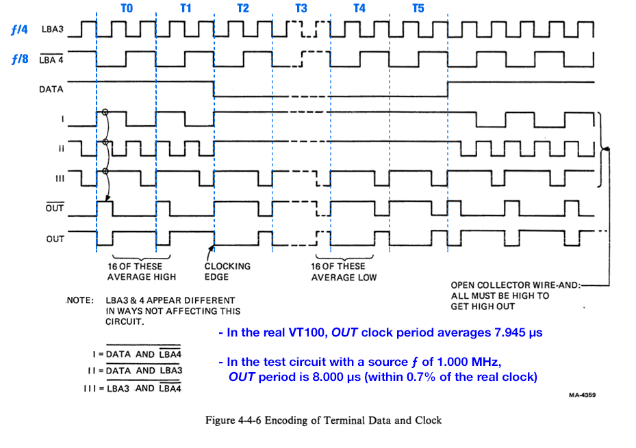
The clocks corresponding to LBA3 and LBA4 are CLOCK_B and CLOCK_C in
my circuit, with periods of 4.0 uS and 8.0 uS, respectively. The
intermediate square waves (I, II, and III) show the logical combination of
the data and the clocks. Finally, the outputs labeled OUT and OUT
represent the clock output on either side of the 7416 buffer/inverter
(because the 7416 is an open collector output, it’s safe to pull it up to
+12V, which is what the interface expects)
I’m just thankful that DEC produced such marvelous documentation. Everything is explained in such great detail. It sure saved me from having to do any actual work, that’s for sure! :^)
Comments